Friday, June 24, 2011

An impression in inside of Kronos

Structure
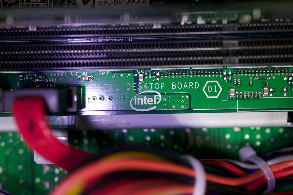
It was not main a motherboard to have been different from my imagination, and a boat of ARM is main / core board. Korg uses ATOM in substitution for DSP. It is the structure such as the conventional synthesizer.
Therefore, I think Korg cannot transplant all on a PC immediately. At least user interface is a reshaping. It may be result working in the ARM side that a sequencer is Legacy. Of course a degree of difficulty is high in acquiring an outside display out.

Time for boot
It takes the time for boot more than 2 minutes. It is necessary for it to shorten it in both ATOM side and ARM side to shorten this. It does not seem to be a problem to be settled if I do something about the ATOM side. For example, even if make DIMM 4GB from 2GB; nonsense. If kronos stores an image of the RAM in SSD and flash memory and boots it, kronos may boot it fast.It is movement such as the hibernation. But a correction of large software / firmware will be necessary. Even if kronos adopted the short OS of the boot-time, It will be hard work for engineers of korg.

Problem of latency
Similarly it is necessary to shorten it in both ATOM side and ARM side. The reason is because one of the causes communicates with ATOM via USB/COM1 between ARM. It may become earlier if Korg uses PCI Express. However, they will not do it from cost. As for the USB, both the price and the technique are stable in an embedded system. As a left method, KORG cannot but improve the software / firmware. Little by little.

An electronic design gets better than I thought
The feeling that korg made hastily does not perform it at all.  There is not the jumper line and sees parts of the Anti-EMI at the minimum, too.  An Electribe was terrible. I want to write it about Electribe sometime.

Kronos is almost comprised of commodity parts
In any kind of electronic equipment parts maker, They can enter musical instrument industry. Korg has opened Pandora's box. Open labs is only the beginning. The thing except electronic parts becomes the entry wall.  For example, a keyboard or patents.

Kronos becomes the physical structure suitable for production in small quantities
The physical structure that is made be production in Japan. I think that there is little number of the production, And Korg cannot make at least kronos in the factory which is low-end.

It is cheap OASYS
I do not know how structure of OASYS turns out, but there is a possibility that Kronos has better performance if OASYS uses the functions such as the videos of the on board. As for OASYS, core Pentium4 2.8GHz single, Kronos is ATOM 1.66GHz dual-core. Judging from a load meter, I seem to assign a synthesizer and an effector to each core.
The comparison of the CPU is this place.
http://www.tomshardware.com/reviews/atom-d510-pentium-4-nettop,2649.html
The outside part including the controller costs money OASYS clearly. I think that it is contents cut down well.


I want to draw a block diagram later.


Kronos内部の感想。

■構造
想像と違ったのはマザーボードがメインではなく、ARMのボートがメイン/コアボードだった。ATOMはDSPの代わりに使っているといえる。従来型のシンセサイザーのような構造だ。
従って、すぐに全てをPC上に移植することはできない。少なくともユーザーインターフェースは作り直しだ。シーケンサーがレガシーなのもARM側で動作しているせいかもしれない。もちろん外部ディスプレイアウトをつけることも難易度が高い。

■ブートの時間
2:10かかると巷では言われている。これを短くするのはATOM側とARM側の両方で短くする必要がある。ATOM側をなんとかすれば解決する問題ではなさそうだ。DIMMを2GBから4GBにしても思ったほど変わらないであろう。
SSDやフラッシュメモリにRAMのイメージごと置いておいてブートすれば速くなるかもしれない。ハイバネーションのような動作。だが大幅なソフトウエア/ファームウェアの修正が必要であろう。外販されているブート時間の短いOSを検討することもできるが、同じように大変であろう。

■レイテンシの問題
同じく、ATOM側とARM側の両方で短くする必要がある。内部をUSBないしCOM1でやりとりしているというのが大きな原因。PCI Expressを使えばもっと早くなるのかもしれないが、コストからやっていないのであろう。組込み系ではUSBは価格も技術もこなれている。
あとは地道なソフトウエア/ファームウェアの改善をしていくしかない。

■設計がこなれている
急いで作った感じがしない。ジャンパやEMI対策部品など。
エレクトライブはヒドかった。いつかこの件に関しては書きたい。

■ほぼ汎用品でできている
やろうと思えばどのメーカーでも参入できる。キーボードや特許など電子部品以外のところが参入障壁だろう。Open labsは始まりに過ぎない。

■もの凄い数を量産するような構造にはなっていない
Made in japanだからできているような構造。生産数もたかが知れていると思う。

■安いOASYSといえる
OASYSの構造がどうなっているか知らないが、もしビデオなどの機能を
使っているとするとKronosの方がパフォーマンスがよい可能性がある。
OASYSはPentium4 2.8GHzシングルコア、KronosはATOM 1.66GHzデュアルコア。
ロードメーターからするとそれぞれのコアにシンセと音源を割り当てているようだ。
CPUの比較はこちら。

コントローラーなど外側の部分は明らかにOASYSの方がお金がかかっている。
うまくシュリンクした内容だと思う。


後ほどブロック図を書きたい。

Tuesday, June 21, 2011

part 5


at one's own risk
  自己責任でどうぞ。


The commentary of the PC part in the left side.
It is a motherboard that is at the left edge.


It is a power supply that is on this side. A yellow cable is connected.
Furthermore, this side, silver thing in the right-side end are SSD.


左手にあるPC部分の解説。
奥にあるのがマザーボード。
その手前にあるのが電源。黄色のケーブルがささっています。
さらにその手前/右端にある銀色のものがSSDになります。

SSD


A fan sticks to a folder of SSD.

SSDのところにファンが付いています。


A power supply unit
電源ユニット

An AC inlet (the part which power supply cord sticks in).
ACインレット(電源コードが刺さる部分)。


A motherboard.
マザーボード。


A memory portion.
1 slot is not crowded.
It leads to SSD in SATA. A red cable of this side.

メモリ部分。
1スロット空いている。
SSDへはSATAでつながっている。手前の赤いケーブル。


The memory is 2GB.
メモリは2GB。

It is made by Intel.
インテル謹製。

Battery.
バッテリ。

As a matter of course, Kronos does not use the audio system interface of the on board.
当然ながらオンボードのオーディオインターフェイスは使っていない。

A cable sticks in a USB terminal.


Kronos does not use the VGA out of the motherboard, and do not seem to output the image with the motherboard as I explained it in part 4.

USB端子にケーブルがささっています。
VGAアウトは使っていません。
part 4で説明したとおりマザーボード側では画像の出力をやっていないようです。


The black cable of the middle is USB. The thing which goes on a front panel when it is a PC.
The PCI slot is empty.

真ん中の黒いケーブルもUSB。PCだとフロントパネルに行くもの。
PCIスロットは空。


A semitransparent connector of the right side is a power supply.
The back connector white small is a fan.

It is slightly incomprehensible, but uses COM1 which is Legacy device when I follow a cable of the slate color!What will kronos use it for?
Possibly do you communicate with the ARM side not USB in COM1?


I really regret that I did not look a little in detail.
But it is troublesome to open out again.


The internal photograph is the end in this.

Reference materials:


右側の半透明のコネクタが電源。
その奥の小さく白いコネクタがファン。

分かりにくいが、ねずみ色のケーブルを辿ると、
レガシーデバイスであるCOM1を使っている!
何に使っているんだろう。
もしかすると、USBではなくCOM1でARM側とやりとりしているのかも。

もう少し詳しく見なかったのを本当に後悔しています。
でもまた開けるのはめんどくさいなぁ。

内部の写真はこれで終わりです。


Sunday, June 19, 2011

part 4

at one's own risk
  自己責任でどうぞ。

The continuance of the story of this board.
There are many mysteries.I regret that I did not check the details.

このボードの話の続き。
謎だらけで、詳細を確認しておけばよかっと後悔しています。


It is the decoding of the part of the left side.
左側のパートの解読です。


What will this daughter board be?
この小基板はなんなんでしょう?


This is an embedded CPU.
A lot of functions are included.
組み込み用CPU。いろいろな機能が入っています。


This is a DRAM.
その下はDRAMです。

NT5TU32M16CG
 DDR2 SDRAM 512Mb


!
Does it lead to an LCD unit from this board?
A lower silver part is an LCD unit.

このボードからLCDユニットにつながっている?
下の銀色の部分が、LCDユニットです。


LCD Unit
UMSH-8240MD-T
 8.0" TFT 800 x 480pixels 250cd/m2  LED Backlight


A questionable point.
1. A CPU is too powerful.
  When say only at frequency; PowerMac G4 class.
  That means, a level to be able to play the simple software synthesizer in itself.
  It is specifications overfor a controller.

2. Why would not korg use the graphic controller of the motherboard?
 Would engineers want to do the CPU of the motherboard side exclusively for a sound?

I am worried about the green daughter board...

ここでの疑問点。
その1 CPUが強力過ぎる。
 周波数だけで言うとPowerMac G4クラス。
 ということはこれ自体でシンプルなソフトシンセができるレベル。
 単なるコントローラーならやり過ぎ。

その2 なぜマザーボードのグラフィックコントローラを使わなかったんだろう。
 マザーボード側のCPUは音専用にしたかったのだろうか。

緑の小基板も気になる。。。


To be continued
続く。

Wednesday, June 15, 2011

part 3

at one's own risk
  自己責任でどうぞ。

The title of today is this board.
Perhaps I think that it is a board making the core.There are many mysteries.
Please point it out if wrong.

本日のお題はこのボード。
恐らく中核をなすボードだと思います。
謎が多いです。
間違っていたらご指摘ください。

The right side is audio system-related roughly, and the left side becomes "embedded" CPU-related.
ざっくり右側がオーディオ関連のパートで、
左側が組み込み用CPUのパートになっています。


Analog Jack board, MIDI board are connected to this board. A white connector and a gray cable are analog. It is a shielded cable.Brown and yellow cables are digital. Do you think that you are all right by the design that so analog wiring and digital wiring are close in? SN ratio etc.

このボードとアナログ・ジャック・ボード、MIDIボードがつながっています。
白いコネクタとグレーのケーブルがアナログ周り。シールドされたケーブルです。
茶や黄色のケーブルたちはデジタル関連。
こんなにアナログとデジタルを近づけて配線して大丈夫なんでしょうか。SNとか。

Three same ICs are DACs.
3つ同じ石がDAコンバーターです。


PCM1793


It is ADC that there is on DACs.
その上にあるのがADコンバーターです。


PCM1802


The small IC of the middle is DIX4192.
真ん中の小さな石がDIX4192。


A right big IC is Flash memory.
右の大きい石がFlashメモリ。
S29AL008J
8 Megabit flash

The left IC is a USB host controller.
その左の石がUSBホストコントローラ。
D720150
USB 2.0 Host or Device Controller


Why will a USB host controller be necessary?
なぜUSBホストコントローラーが必要なんだろう?


To be continued.
続く。


Sunday, June 12, 2011

part 2

at one's own risk
自己責任でどうぞ。


When I took the board of MIDI. It can be stood with tape.
I comment;
The lower right is an analog Jack board
The lower center is a panel board.
The left brown board is for keyboards.
The top of the analog Jack board is broadcast boards such as the USB. AD/DA appears here, too.It is a core-like board.
The upper silver part is SSD and an LCD unit.
The upper is a power supply unit.
The top is a motherboard.

MIDIの基板をとったところ。テープで立ててあります。
解説すると、右下がアナログのジャック基板、中下はパネル基板。
左の茶色の基板はキーボード用。
アナログジャック基板の上がUSBなどの中継基板。ここにAD/DAなども載っています。
中核的な基板です。
その上の銀の部品はSSDとLCDユニット。
その上が電源ユニット。
更にその上がマザーボード。


Before taking the MIDI board,The signal from joy-stick and a keyboard is in the MIDI board once, too.
MIDIのボードを取る前。ジョイスティックやキーボードからの信号も一旦MIDIのボードに入ります。


A close-up
クローズアップ。

After I took the MIDI board. There is not the painting of a part coming in contact with a body.The reason will be because it drops GND. electric wave?
MIDIボードをとったところ。留める部分の塗装がありません。GNDを落とすためでしょうね。

The analog Jack board. OPAMP is N5532A.
アナログのジャックボード。オペアンプはN5532A。


A black IC in the right of a gray cable seems to be the amplifier of headphones.
灰色のケーブルの右にある黒い石がヘッドホンのアンプと思われる。


To be continued
続く。